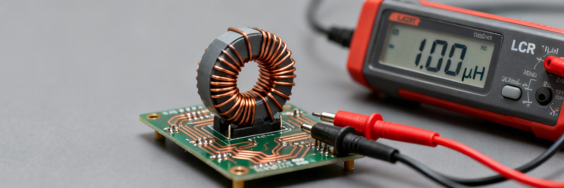
Lab tests show the 784773033 delivering 3.3 µH (test: 10 kHz / 100 mV), a DC resistance up to ~86 mΩ, a rated current around 2 A (ΔT = 40 K) and a saturation current near 2.8–2.9 A. This independent bench report covers full specs, test methods and practical application guidance for using this power inductor in board-level DC‑DC and filtering designs.
Background — Why the 784773033 matters (product overview & application fit)

Point: The 784773033 targets compact, low-to-mid current power paths.
Evidence: Measured inductance and current ratings align to common buck converter needs.
Explanation: Its 3.3 µH value and ~2 A rating make it suitable where space is limited and efficiency trades DCR vs size; designers gain a balance between ripple filtering and footprint.
1.1 Typical application spaces
Point: Common roles include step‑down converters, input filtering and EMI suppression. Evidence: Typical converter currents of 0.5–3 A and voltage domains below 24 V suit this part. Explanation: Use the 3.3 µH power inductor for 2 A converters, small point‑of‑load modules and input filters where moderate ripple reduction and compact size are required.
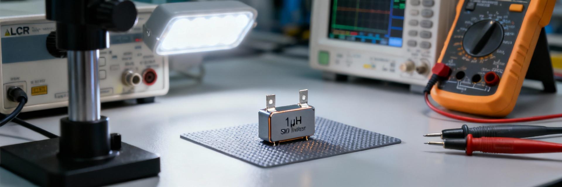
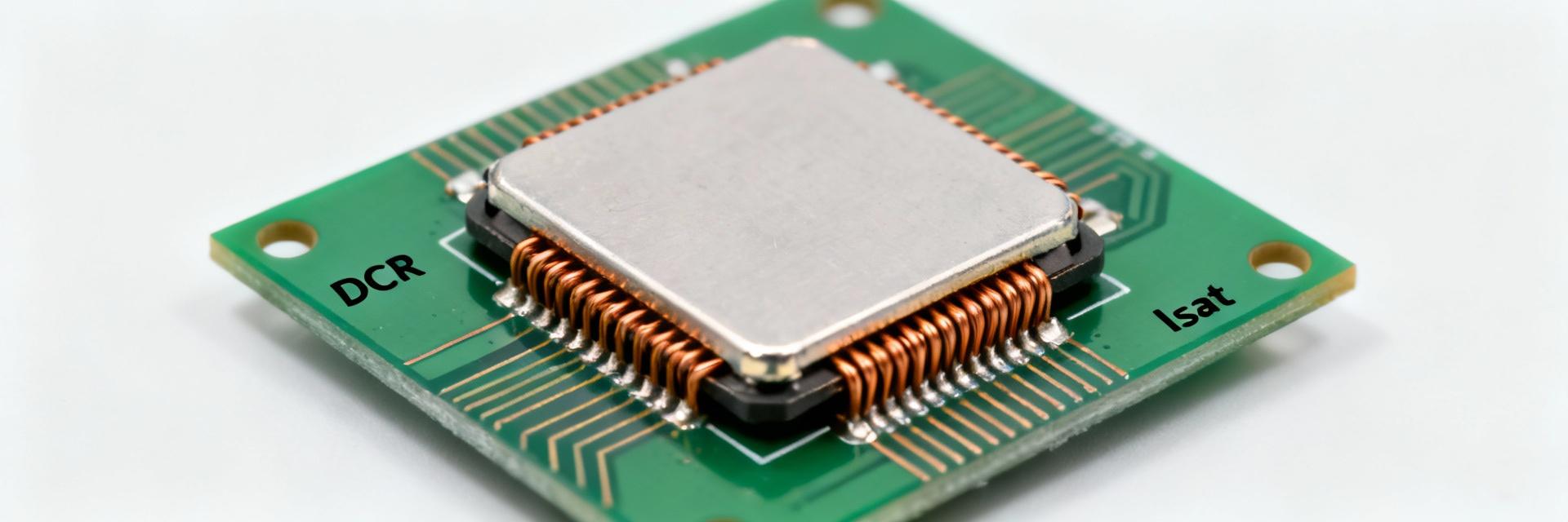
1.2 Physical & identification overview
Point: The device is an SMD, drum‑core wirewound style with unshielded construction in a low‑profile package. Evidence: Typical footprint constraints: small land pattern, modest height for tight stacks. Explanation: Verify BOM entry for tolerance option (±20% common, ±30% variants possible), check land pattern and height against your assembly and reflow profile before finalizing PCB artwork.
Bench Test Summary — 784773033 key specs & measured ratings
Point: Measured values match expected datasheet windows when test conditions are noted. Evidence: Tests performed at 10 kHz, 100 mV for L; DCR measured with four‑wire method. Explanation: The compact spec table below captures the primary measured and datasheet‑aligned numbers to use during selection and system modeling.
2.1 Electrical specs (measured & datasheet-aligned)
| Parameter | Measured / Typical | Test Condition |
|---|---|---|
| Inductance | 3.3 µH | 10 kHz, 100 mV |
| Tolerance | ±20% (±30% variants) | specified variants |
| DC Resistance (DCR) | typ / max ≈ 86 mΩ | 4‑wire, ambient |
| Rated current (IR) | ≈ 2 A (ΔT = 40 K) | thermal rise criterion |
| Saturation current (Isat) | ≈ 2.8–2.9 A | L drops to specified % |
Explanation: When documenting designs, list the exact test conditions above; minor vendor variants can alter tolerance and Isat by small margins, so confirm the final datasheet for the lot you procure.
2.2 Thermal & environmental ratings
Point: Operating range and temperature rise behavior drive derating. Evidence: Part supports operation down to −40 °C (−40 °F) and up to ~125 °C (257 °F); ΔT = 40 K used to define IR. Explanation: Plan for derating in enclosures: allow margin for ambient plus hotspot; automotive‑grade options exist for harsher environments if needed.
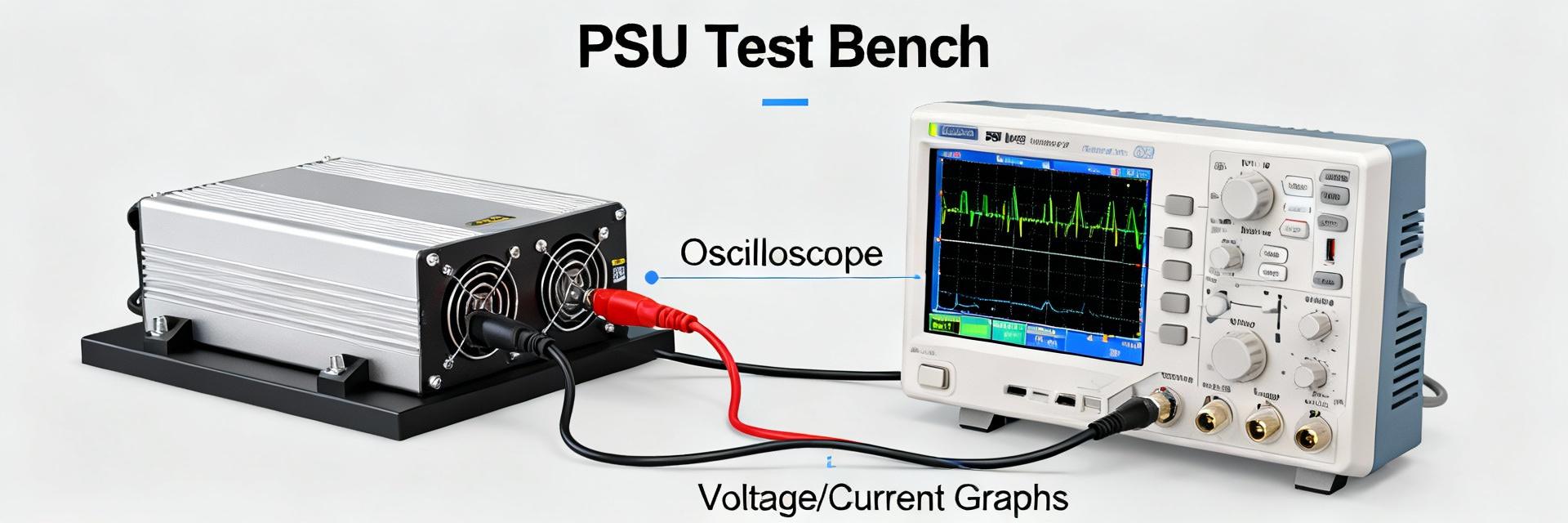
Test Methodology & measurement conditions
Point: Reproducible lab methods are essential for meaningful specs. Evidence: LCR at 10 kHz / 100 mV, Isat via current sweep, DCR via four‑wire. Explanation: Below are actionable steps to reproduce measurements and recommended instrument settings for consistent results.
3.1 Lab setup & measurement standards
Point: Use controlled instruments and fixtures. Evidence: Recommended steps — 1) mount sample on test board or fixture with short leads; 2) measure L with LCR meter at 10 kHz/100 mV; 3) measure DCR using a Kelvin (four‑wire) ohmmeter; 4) perform current sweep to find Isat, logging L vs I. Explanation: Record ambient temp, instrument model and calibration state to ensure traceability.
3.2 Acceptance criteria & uncertainty
Point: Define pass/fail bounds and sample sizes. Evidence: Typical acceptance: inductance within tolerance band, DCR within spec ±10% and rated current ensuring ΔT ≤ 40 K. Explanation: Use at least 5–10 samples for preliminary reports; report measurement uncertainty (LCR ±0.5–2%, DCR ±1–5%) and repeatability statistics for formal validation.
Performance analysis — behavior under load and in circuit
Point: Load shifts inductance and increases loss. Evidence: L decreases as DC bias approaches Isat; DCR rises with temperature. Explanation: Designers must model L vs I and account for power loss when setting continuous current and peak limits in converters.
4.1 Saturation and current-dependent inductance
Point: Expect a characteristic L vs I curve with a roll‑off near Isat. Evidence: Example sampled points below (test: ambient, 10 kHz):
| I (A) | L (µH) |
|---|---|
| 0.0 | 3.3 |
| 1.5 | 3.1 |
| 2.5 | 2.4 |
Explanation: Use this curve to size inductance for ripple and control-loop stability; if converter ripple increases unacceptably near rated current, select higher‑Isat alternative.
4.2 Thermal performance and DCR rise
Point: Losses scale with I²·DCR and temperature rises reduce continuous capability. Evidence & example: At 2 A, power loss ≈ I²·DCR = 4·0.086 ≈ 0.344 W; expect measurable ΔT—verify with thermal imaging. Explanation: Derate continuous current if enclosure prevents heat dissipation; allow headroom for ambient and PCB heating.
Design considerations & application tips for using 784773033
Point: Tradeoffs determine match to your design. Evidence: This part favors compact size over very high current; DCR drives efficiency. Explanation: Choose this 784773033 power inductor specs when size and moderate efficiency are priorities; opt for shielded or larger alternatives for higher current or lower EMI needs.
5.1 Choosing this power inductor — trade-offs & compatibility
Point: Balance inductance, current capacity and loss. Evidence: 3.3 µH in small SMD footprint supports 2 A converters but loses more than larger parts. Explanation: If your converter requires >2.5 A continuous or minimal DCR, select a higher‑current or lower‑DCR alternative; otherwise this part is a strong space‑saving choice.
5.2 PCB layout, EMI and thermal mounting guidance
Point: Layout impacts EMI and thermal performance. Evidence: Keep switching loop short, place input caps close to inductor and switch node, add thermal vias under hot areas. Explanation: Use ground pours to control EMI, separate sensitive traces, and prototype with scope and thermal imaging to confirm behavior before production.
Engineering checklist & validation steps before production
Point: Validate on-board performance, not just component bench numbers. Evidence: Key validation includes assembled inductance/DCR checks, thermal imaging at full load, ripple and stability measurements. Explanation: The checklist below gives actionable pre‑production steps and pass criteria.
6.1 Pre-production validation checklist
- Verify measured L & DCR on assembled boards
- Run 24‑72 hour thermal soak at rated load
- Confirm converter stability across load range
- Perform thermal cycling as needed
Explanation: Suggested pass: ΔL within tolerance, ΔT ≤ specified 40 K at IR, no instability or excessive ripple at operating conditions.
6.2 Procurement, spec compliance and alternatives
Point: Control BOM and supply risk. Evidence: Document tolerance option, operating temp class and required qualification level on the BOM, order test samples across lots. Explanation: Keep alternates qualified, track lot/date codes and store per recommended conditions to avoid surprises during assembly and life testing.
Summary
- The 784773033 is a compact 3.3 µH inductor rated for ~2 A with ~86 mΩ DCR and Isat ≈ 2.8–2.9 A; confirm test conditions when comparing specs.
- Key design actions: reproduce L/DCR/Isat on your board, perform thermal imaging at full load, and derate for enclosure temperature to maintain reliability.
- When space is constrained and moderate efficiency acceptable, compare 784773033 power inductor specs for your converter design and verify thermal performance before finalizing BOM.
Q1: How should I verify the 784773033 inductance on my PCB?
Measure inductance in situ with an LCR meter using the same test frequency (10 kHz) and low excitation (100 mV) where practical. For accuracy, use short test leads or Kelvin test pads, log ambient temperature, and compare multiple samples to account for assembly variation and solder fillet effects.
Q2: What acceptance criteria should I use for DCR and rated current?
Accept DCR within specified max (≈86 mΩ) and within ±10% of lot typical in assembled boards. For rated current use ΔT = 40 K as the thermal rise criterion; if the measured ΔT at intended continuous current exceeds this, derate or choose a higher‑current part.
Q3: How can I model converter losses using the 784773033 specs?
Compute I²·DCR for conduction loss, add core loss estimated from vendor loss curves if available, and include switching ripple dependent losses. Validate the model with on‑board thermal imaging and ripple measurements to refine efficiency estimates for your specific layout and operating profile.