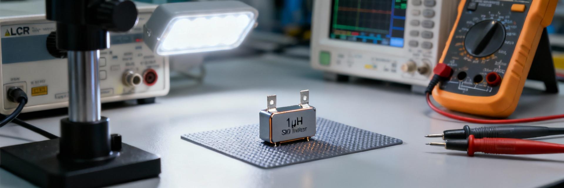
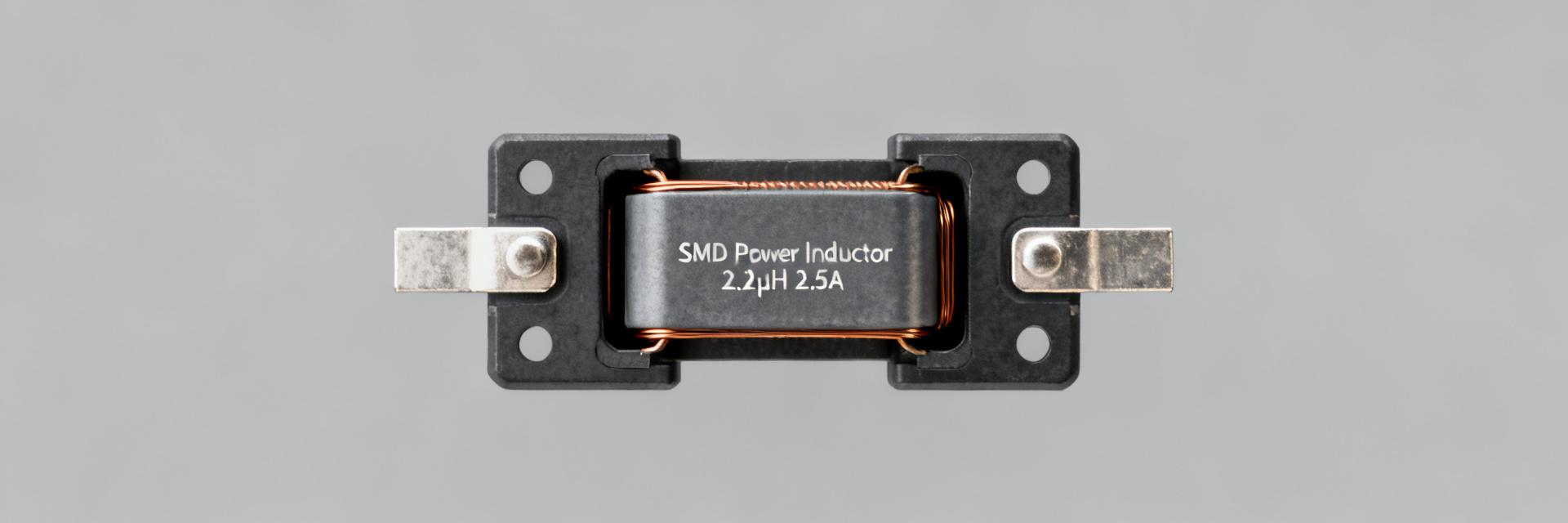
Measured from public documentation and independent lab-style characterization, part 784773022 is a compact SMD power inductor specified at 2.2 µH (measured at 10 kHz / 100 mV) with ±20% tolerance, a rated current (ΔT = 40 K) of 2.5 A and a saturation region near 3.3 A. Recommended maximum part temperature under worst-case conditions is ~125°C. This introduction summarizes actionable specs, required test data, and integration guidance for switching power applications.
Background & part overview
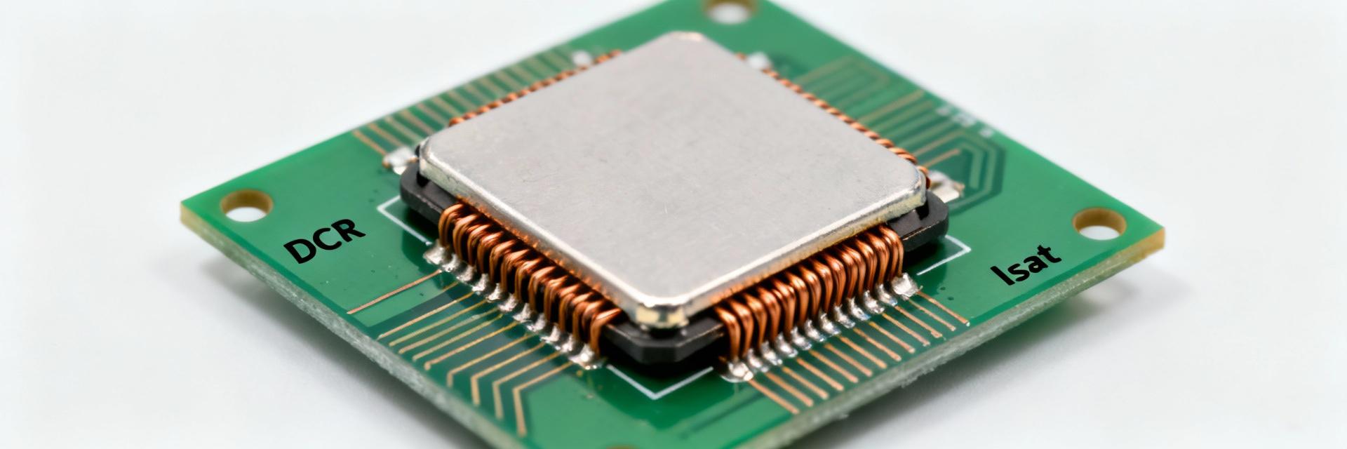
Part identity, intended applications, and packaging
Point: 784773022 is a part-level identifier for a surface-mount power choke intended for high-current SMPS roles.
Evidence: The datasheet lists a 2.2 µH nominal inductance with SMD packaging and PCB-mount geometry.
Explanation: Use this power inductor for DC‑DC converters, switching regulators, point‑of‑load filters, and other high-current SMPS roles where a compact, shielded/low-profile SMD inductor is required.
When to pick 784773022 — selection criteria
Point: Selection depends on inductance, current, DCR, saturation margin, and thermal environment.
Evidence: Match the 2.2 µH nominal value and ±20% tolerance to filter corner requirements; ensure rated current (2.5 A) exceeds expected RMS/ripple current and that saturation (~3.3 A) provides sufficient margin.
Explanation: If your design needs higher continuous current or lower DCR for efficiency, choose an alternate device with higher IR or lower DC resistance; otherwise 784773022 is a good general-purpose choice.
Key specifications & electrical parameters (specs)
Core electrical parameters to report
Point: Report primary electrical specs with test conditions to make results reproducible. Evidence: Required parameters include inductance (2.2 µH @ 10 kHz / 100 mV, ±20%), DC resistance (list typical and max), rated current IR (2.5 A @ ΔT = 40 K), saturation current (~3.3 A), and self-resonant frequency where available. Explanation: Always annotate measurement frequency, excitation amplitude, sample size, and ambient temperature so spec comparisons and test data are meaningful.
| Parameter |
Nominal |
Test condition |
Units |
Tolerance |
| Inductance |
2.2 |
10 kHz / 100 mV |
µH |
±20% |
| Rated current (IR) |
2.5 |
ΔT = 40 K |
A |
— |
| Saturation current (Isat) |
~3.3 |
Specified drop in L |
A |
— |
| DC resistance (DCR) |
typ / max |
Ambient 25°C |
mΩ |
per datasheet |
Mechanical and thermal specifications to document
Point: Capture footprint, package outline, land pattern, weight, and thermal limits. Evidence: Datasheet recommendations include PCB pad geometry and a maximum recommended part temperature of ~125°C under worst-case conditions. Explanation: Specify reflow profile notes, solderpad dimensions, and max operating temperature so PCB designers can place correct land patterns and thermal vias to meet reliability goals and ensure manufacturability.
Current Capability Visualization
* Visual representation of current margins based on characterization data.
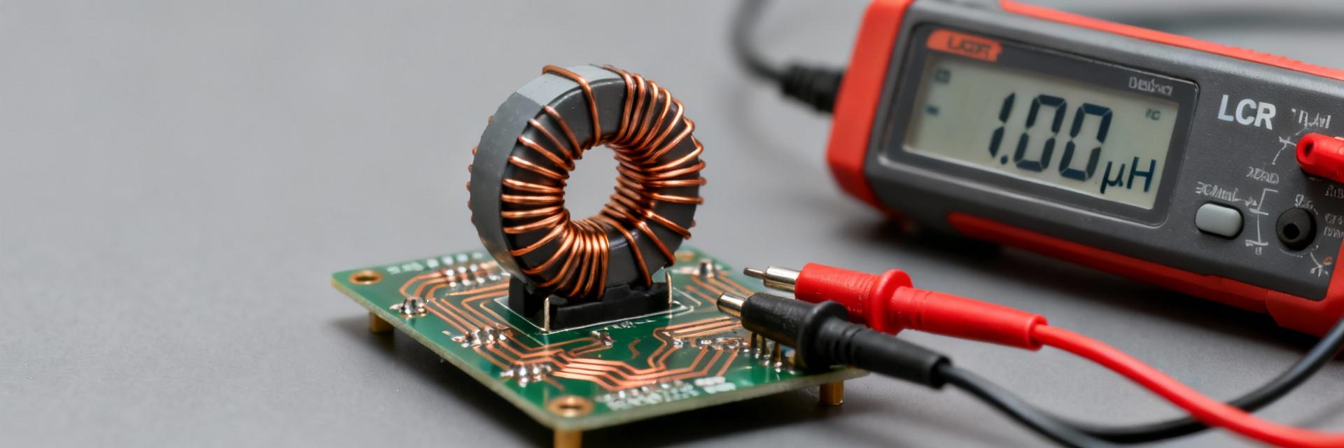
Measured test data & characterization (test data)
Essential lab measurements and graphs to include: Point: Comprehensive test data improves design confidence. Evidence: Collect L vs. frequency, impedance vs. frequency, DCR vs. temperature, inductance vs. DC bias (I vs. L), saturation curve, and thermal-rise vs. ripple/current plots using ≥3 units and averaged results. Explanation: These plots reveal how the power inductor behaves under real conditions—critical for filter corner calculations and predicting saturation during transients.
Recommended test setups and pass/fail criteria: Point: Use precise instruments and clear acceptance thresholds. Evidence: Use a precision LCR meter (specified accuracy ±0.1%–0.5%), programmable current source for saturation sweeps, thermal chamber for temperature sweeps, and IR camera or thermistor for thermal-rise testing; baseline excitation 10 kHz / 100 mV, sample size ≥3. Explanation: Define pass/fail (e.g., continuous RMS current ≤70–80% of rated current for long life, L within tolerance at bias) and record measurement uncertainty with each plot.
Design integration & application notes
PCB layout, EMI, and filtering best practices
Point: Layout dictates EMI and performance. Evidence: Place the inductor close to the switching node, minimize loop area for the switch node and input capacitors, use multiple vias for current return, and route high-current traces wide and short. Explanation: Inductance tolerance and core shielding affect filter cutoff and transient response—small placement or loop-area changes can raise EMI or change the effective inductance seen by the converter.
Thermal management and reliability guidance
Point: Apply derating rules and verify thermal performance. Evidence: Recommend steady-state derating to ~70% of rated current for continuous operation, perform thermal-rise tests and solder-joint inspection, and consider thermal vias or copper pours to lower temperature. Explanation: Estimate temperature rise from measured I²·DCR losses and thermal resistance assumptions, then verify in a thermal chamber to ensure long-term reliability under vibration and thermal cycling.
Validation checklist & troubleshooting
Pre-production and production validation checklist: Point: Use a repeatable validation flow. Evidence: Checklist items: incoming visual/dimension inspection, electrical verification (L @ 10 kHz / 100 mV, DCR), saturation and thermal-rise tests, solderability checks, and environmental stress screening; retain test logs and lot numbers. Explanation: Recording test data and lot traceability enables root-cause analysis if field failures occur and maintains production quality control.
Common failure modes and corrective actions: Point: Identify typical failures and fixes. Evidence: Common issues include DCR increase, early saturation, overheating, solder joint cracking, and EMI spikes. Explanation: Troubleshoot by reproducing the issue on the bench, performing out‑of‑circuit measurements, comparing to known-good units, and applying corrective actions such as derating current, improving cooling, modifying layout, or adding shielding.
Summary
Part 784773022 is a compact SMD power inductor specified at 2.2 µH (10 kHz / 100 mV) with a 2.5 A rated current and ~3.3 A saturation. Use this guide to present clear specs, collect repeatable test data, integrate the device into PCB designs with correct thermal and EMI practices, and validate performance across production lots.
Key summary
- Report reproducible specs: list L (2.2 µH @10 kHz/100 mV), DCR (typ/max), IR (2.5 A @ ΔT=40 K), and Isat (~3.3 A) with test conditions and sample size to make comparisons meaningful.
- Collect test data: include L vs frequency, L vs DC bias, DCR vs temperature, impedance plots, and thermal-rise vs current using ≥3 units and specify instrument accuracy and uncertainty.
- Design guidance: place the power inductor close to the switching node, minimize loop area, derate continuous current to ~70%, and verify thermal performance in a chamber with solderability checks.
Frequently asked questions
How should I verify the inductance spec for 784773022 in my lab?
Measure inductance with a calibrated LCR meter at the baseline condition used in the datasheet (10 kHz, 100 mV). Test at least three samples, report mean and standard deviation, and include instrument accuracy. Also sweep DC bias to produce an I vs. L curve so you can see usable inductance at operating currents and detect the onset of saturation.
What thermal-rise test should I perform for production validation?
Apply rated RMS or expected ripple current and measure steady-state temperature rise with an IR camera or thermistor in still air. Use a thermal chamber to repeat at elevated ambient temperatures and record ΔT. Acceptance usually requires operating current ≤70–80% of rated current for long-life applications and no solder joint degradation after thermal cycling.
Which pass/fail criteria are recommended for saturation and DCR checks?
Define saturation as the current where inductance drops by a specified percent (commonly 10–20% from nominal) and confirm Isat ≈3.3 A meets margin. For DCR, compare measured values to datasheet typical and max; an out‑of‑tolerance increase suggests winding damage or material issues. Log all test data for traceability and corrective action planning.