Introduction: Recent industry audits and designer surveys attribute roughly 20–30% of power-stage assembly and field reliability failures to incorrect SMD inductor footprint geometry and related process choices. This report delivers a compact, data-driven playbook for designing reliable footprints, sizing pads, specifying manufacturing and electrical tolerances, and validating layouts before production to reduce rework and protect power-stage performance.
The guidance below targets PCB designers and DFM engineers working on high-current power stages. It blends practical heuristics, process-aware tolerances, and pre-production checks that can be run with typical board-house capabilities and AOI workflows. Use the pad tables and checklist to accelerate review cycles and catch footprint-rooted defects before NPI volumes.
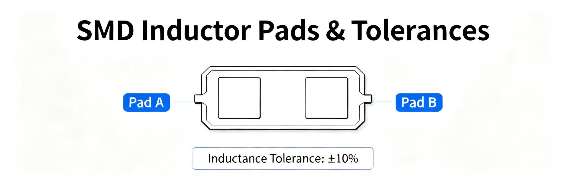
Why the SMD inductor footprint matters — background
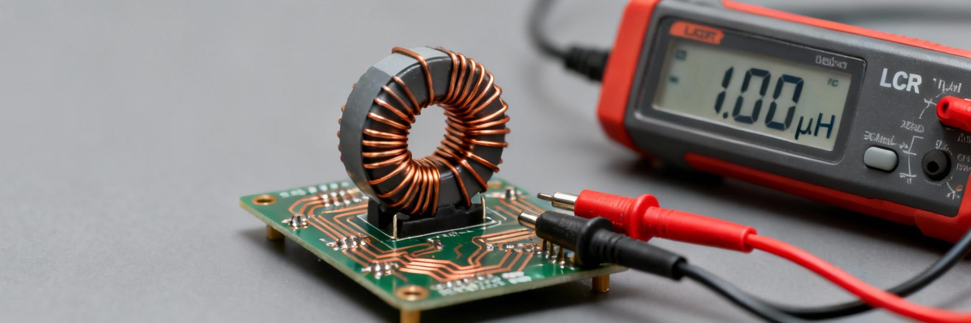
Role in electrical performance and reliability: Footprint geometry directly affects solder joint quality, stray inductance, thermal dissipation, and current handling. A marginal pad-to-terminal overlap raises joint impedance, increases DCR under thermal stress, and shifts stray inductance enough to alter switching-node performance. Designers should track failure modes such as lift, cold joints, and unexpected DCR rise when footprints are undersized or misaligned with terminal metallurgy and plating.
Role in electrical performance and reliability
Reliability evidence: poor geometry yields weak fillets and uneven solder wetting, which show up as elevated contact resistance or intermittent connections under vibration. Practical checkpoints: verify solder fillet continuity, confirm fillet height visually or via AOI, and measure initial DCR on first articles. Documenting these checks closes the loop between footprint choices and electrical performance during burn-in and thermal soak tests.
Common failure modes traced to footprint mistakes
Typical problems include tombstoning, insufficient solder fillet, pad spattering, and mechanical detachment under vibration. Symptoms seen in the field: intermittent high-side switching, elevated hot-spot temperatures near terminals, or mechanical separation after thermal cycling. Inspection checks: fillet coverage on both terminals, absence of solder balls near pads, and AOI-programmed fillet geometry tolerances to flag weak joints prior to reflow qualification.
Industry data & trends impacting footprints (data analysis)
Field and manufacturing statistics (what the numbers show): recent manufacturing audits show footprint-related issues remain a meaningful fraction of assembly defects, especially as power inductors grow in current rating and footprint complexity. Yield losses attributed to footprint errors concentrate in reflow-related defects and part mismatches.
Field and manufacturing statistics
| Root cause | % defects (typical) |
|---|---|
| Assembly process (misplacement, solder paste) | 45% |
| Footprint & pad design | 25% |
| Part mismatch / datasheet error | 15% |
| Other (handling, materials) | 15% |
Implications for modern power designs and automated assembly
Smaller pitches, higher currents, and aggressive AOI increase the consequences of marginal pad choices. Conservative pad choices improve yield but consume board area; the trade-off must be quantified early. For automated assembly, specify paste aperture and mask features that produce predictable fillet geometries within AOI thresholds to minimize false fails and rework loops.
Pad sizes: how to calculate and reference dimensions
Inputs and formulae for pad-size calculation: start from the component terminal bounding box (L×W), add manufacturing tolerances for copper etch and registration, then choose a nominal pad-to-terminal overlap (commonly 0.5–1.0× terminal width per side for power terminals). Account for solder fillet by sizing the pad slightly longer than the terminal.
Heuristic Formulas
- Pad Length = Terminal Length + 0.02–0.05 in (20–50 mil)
- Pad Width = Terminal Width + 0.01–0.03 in
- Paste Coverage = 60–80% of land area
Recommended pad-size ranges
| Part class | Pad (L×W) mil | Paste % |
|---|---|---|
| Small chip (0805-style) | 120×80 | 60–70% |
| Mid-size power (1210–1812-style) | 160–220 × 100–140 | 65–75% |
| Large high-current SMD | 240–360 × 140–220 | 70–80% |
Tolerances: fabrication, assembly, and electrical limits
Include copper plating, etch, and registration variation when defining pad outlines and courtyard. Typical safe bands: ±5–10 mils (±0.13–0.25 mm) for pad outline and ±5–15 mils for courtyard depending on board house capability.
PCB fabrication and assembly tolerances
Specify pad expansion/contraction expectations and communicate target solder mask clearance to avoid mask slivers at pad edges. When in doubt, include slightly larger mask openings on high-current pads to ensure reliable fillet formation.
Electrical and thermal tolerances
Footprint choices impact current density and thermal conduction to the board. For high-current inductors derate the copper cross-section adjacent to the terminal or add thermal vias outside the pad to spread heat. Specify acceptable DCR drift under thermal load (for example ≤X% at rated current).
Layout and assembly best practices
Solder mask, paste, and fillet best-practices
Recommended paste percent: 60–80% depending on pad size and terminal height. Ensure stencil thickness and aperture design are communicated to assembly to control solder volume. Target AOI fillet acceptance criteria and program AOI accordingly.
Placement, clearance, and routing
Place inductors close to switching MOSFETs and sense resistors to minimize loop area; route high-current traces with multiple ounces of copper or wider traces, and provide robust return vias. Use via-in-pad selectively for thermal needs but beware of solder wicking; prefer via-near-pad when thermal spread is needed.
Examples, validation, and a pre-production checklist
Three annotated footprint examples
| Example | Pad (mil) | Paste |
|---|---|---|
| Small chip | 120×80 | 65% |
| Mid-size power | 200×120 | 70% |
| Large high-current | 320×180 | 75% |
Pre-production validation checklist
- Verify datasheet terminal dimensions
- Run footprint DRC vs IPC-equivalent rules
- Print first-article boards
- Confirm fillet wetting and AOI acceptance
- Perform thermal-rise test at rated current
Summary
A correct SMD inductor footprint—sized pads with documented tolerances—reduces assembly defects, improves current and thermal performance, and lowers rework cost. Follow a disciplined approach: validate mechanical dimensions, apply pad-size calculations, and run the pre-production checklist to confirm results prior to volume production.
Key summary
- Design pad sizes from actual terminal dimensions, add process overlays, and select paste coverage to control fillet formation.
- Specify fabrication and assembly tolerances (pad outline ±5–10 mil typical) to avoid production surprises.
- Use AOI-targeted fillet metrics and thermal-rise testing to validate footprints and prevent field failures.
Common questions & answers
How does an SMD inductor footprint affect thermal performance?
Pad area and adjacent copper influence thermal conduction away from the terminal; larger pads with additional copper pours and thermal vias reduce hotspot temperature. Validate with a thermal-rise test at rated current to confirm the design.
What pad sizes and tolerances should I use for a mid-size power inductor?
For mid-size power inductors, start with pad lengths 0.02–0.05 in longer than terminal length and pad widths 0.01–0.03 in wider than terminal width, and use 65–75% paste coverage. Specify fabrication tolerances of ±5–10 mil for pad outlines.
How can I verify my SMD inductor footprint before full production?
Run a DRC against IPC-equivalent rules, produce first-article boards, inspect fillet quality with AOI and manual inspection, measure initial DCR and perform thermal-rise testing at rated current, and iterate the pad or paste apertures as needed.