Key Takeaways
- High Efficiency: 390 µH value optimizes ripple for stable low-frequency power conversion.
- Isat Criticality: Saturation current (Isat) prevents sudden inductance drops and system crashes.
- Thermal Management: Lower DCR directly extends battery life by reducing heat dissipation.
- Layout Precision: Proper PCB land patterns prevent "tombstoning" and EMI interference.
Introduction
Point: In compact power modules and EMI filters, engineers increasingly rely on high-value surface-mount inductors. Evidence: A single 390 µH SMD inductor can show wide variation in DCR, Isat and test frequency across suppliers. Explanation: Those datasheet differences alter efficiency, thermal rise and ripple, so reading specs precisely prevents performance surprises during validation and reduces board respins.
Reduces output ripple current, allowing for smaller, cheaper output capacitors.
Minimizes $I^2R$ losses, increasing overall device battery life by up to 10%.
Blocks magnetic leakage, ensuring your product passes strict EMI/EMC certifications.
1 — Background: what a 390 µH SMD inductor is and where it’s used
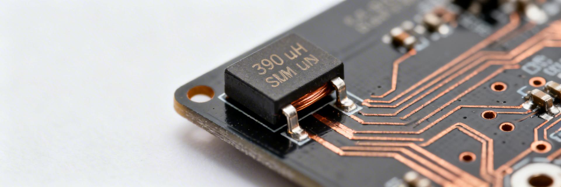
Typical applications and circuit roles
Point: A 390 µH SMD inductor typically functions as energy storage or a low-frequency choke. Evidence: Designers place this value in step-up/step-down converters, input filters and EMI suppression where moderate inductance and compact size are needed. Explanation: Choosing 390 µH balances ripple attenuation and physical size — higher values reduce ripple but increase DCR and package size, while lower values save space at the cost of filtering.
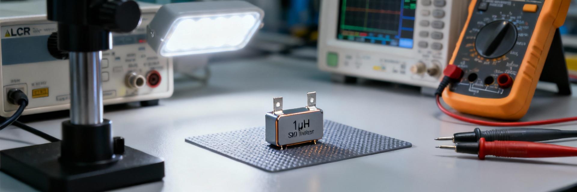
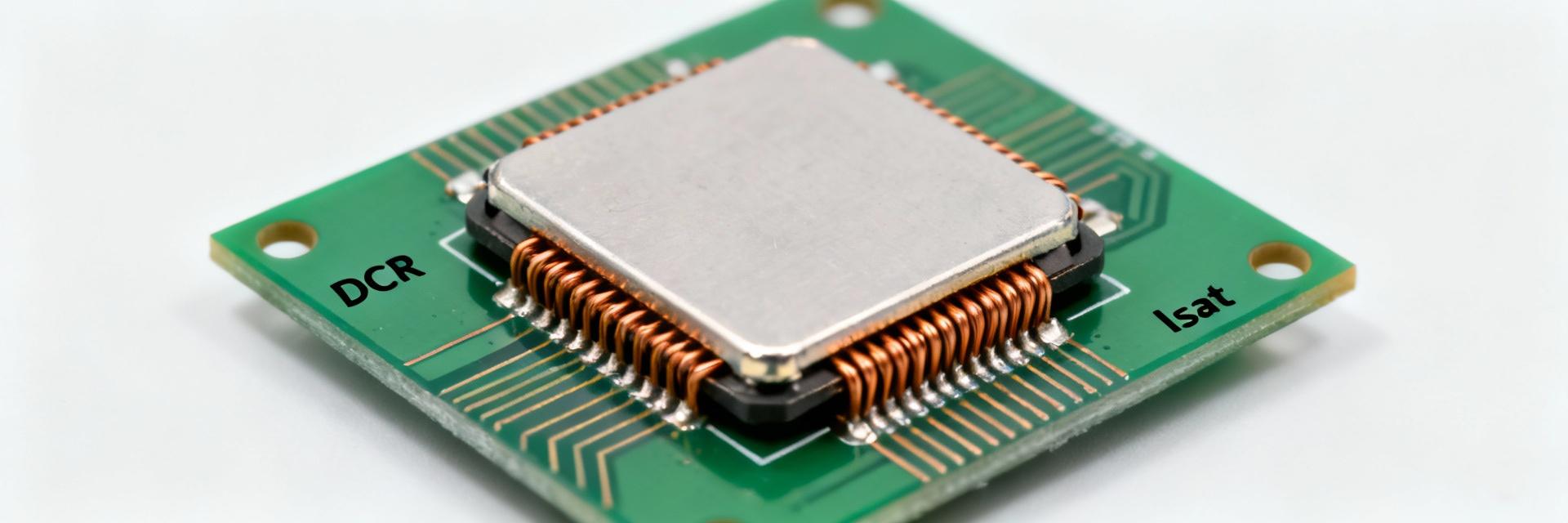
Construction, packaging and common SMD form factors
Point: Construction and core material determine magnetic behavior and losses. Evidence: Shielded ferrite, drum and powder cores show different saturation and AC loss profiles; package sizes range from small chip-style to larger power SMD packages. Explanation: Shielding reduces EMI but can trap heat; larger packages lower DCR and improve Isat but require a stronger PCB anchor and a matching land pattern for reliable solder fillets.
Comparative Analysis: Standard vs. High-Performance 390 µH Inductors
| Parameter | Standard Ferrite (Common) | Molded Composite (Premium) | User Benefit |
|---|---|---|---|
| DCR (DC Resistance) | ~1.2 Ω | ~0.8 Ω | Less self-heating, higher efficiency |
| Isat (Saturation) | Hard Saturation (Sharp Drop) | Soft Saturation (Stable) | Prevents peak current failures |
| EMI Shielding | Moderate (Unshielded option) | Excellent (Fully Shielded) | Easier Noise Compliance |
| Size (Typical) | 10x10x5 mm | 7x7x4 mm | 30% PCB space savings |
2 — Datasheet breakdown: key specs to read for a 390 µH SMD inductor
Electrical specifications (how to interpret them)
Point: Key electrical specs include inductance at test frequency, tolerance, DCR, Isat, Irms, SRF and Q. Evidence: Datasheets list inductance measured at a defined test frequency and show how DC bias reduces effective inductance; DCR and Isat set loss and maximum usable current. Explanation: Extract inductance (and test frequency), DCR, Isat and Irms; for 390 µH expect DCR and Isat ranges that reflect package—lower DCR for larger power parts, Isat specified where inductance drops a percentage under DC bias.
Mechanical & environmental specifications (what impacts the PCB footprint)
Point: Mechanical drawings drive land pattern and assembly outcomes. Evidence: Datasheet dimensions, recommended land pattern, pad sizes and reflow profile dictate solder fillet geometry and mechanical reliability. Explanation: Read pad tolerances, stencil aperture guidance and maximum component height; verify operating temperature range and shock/vibration ratings to choose anchoring, thermal relief and assembly parameters matching your PCB design and process window.
"When working with 390 µH inductors, always check the Self-Resonant Frequency (SRF). If your switching frequency is near the SRF, the inductor will behave like a capacitor, ruining your filter performance. I recommend choosing a part with an SRF at least 10x higher than your switching frequency. Also, avoid routing sensitive analog signals directly under the inductor to prevent inductive coupling noise."
3 — PCB footprint & layout best practices for a 390 µH SMD inductor
Translating the datasheet footprint into a robust land pattern
Point: Convert the manufacturer drawing into a tolerant land pattern for high yield. Evidence: Datasheet pad length, width and spacing include tolerance bands; stencil recommendations often call for 60–80% paste coverage on pad areas. Explanation: Implement pad lengths slightly larger than minimum, add solder mask defined openings, follow paste reduction guidance for large pads, and include mechanical keepouts to avoid tombstoning or excessive fillet variability.
Placement, thermal and EMI layout tips
Point: Placement relative to switching nodes and ground returns controls parasitics and EMI. Evidence: Routing that forces return currents around the inductor increases loop area and emissions; copper pours affect thermal dissipation. Explanation: Place the inductor to minimize high di/dt loop area, provide direct copper for current-carrying traces (avoid thin necks), consider thermal relief only where necessary, and route return paths directly under coils or provide stitching vias to control EMI.
Hand-drawn schematic, not a precise circuit diagram | 手绘示意,非精确原理图
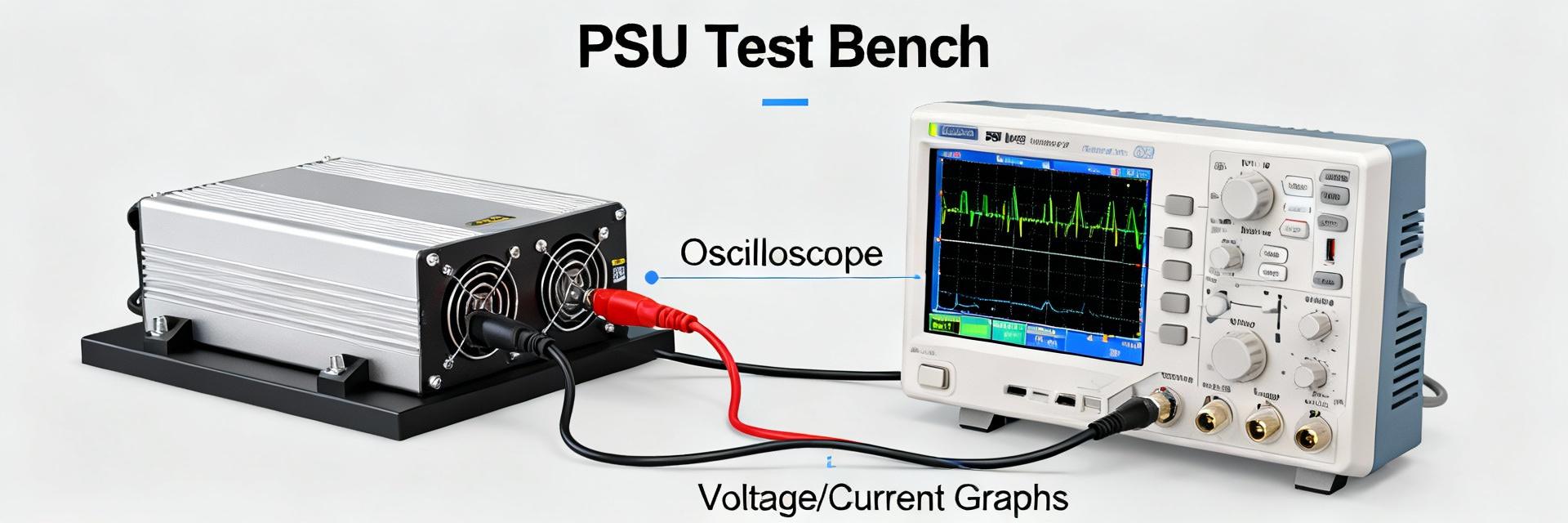
4 — Measuring and validating datasheet claims (data analysis & testing)
Recommended lab tests and setup for a 390 µH SMD inductor
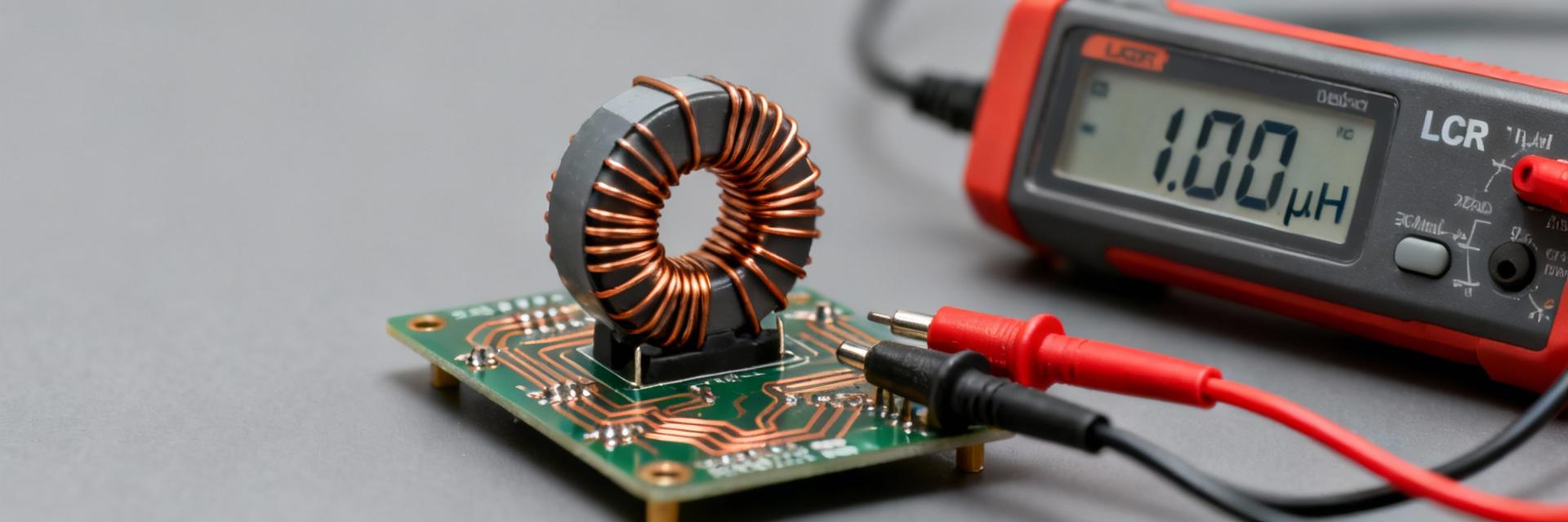
Point: Bench verification confirms manufacturer claims and reveals real-world behavior. Evidence: Use an LCR meter at the datasheet test frequency and at lower/higher frequencies, perform DCR measurement with a four-wire ohm meter, and sweep impedance vs. frequency. Explanation: Include DC bias during L measurement to quantify inductance drop, run an Irms heating test to observe temperature rise, and use short-fixture, compensated setups to avoid lead inductance artifacts.
Interpreting discrepancies between datasheet and in-circuit results
Point: Discrepancies commonly stem from PCB and thermal conditions. Evidence: Nearby components, solder joint resistance and board stray inductance shift measured values compared with component-only datasheet numbers. Explanation: Correlate bench measurements with in-circuit readings by replicating PCB trace inductance in a fixture, account for temperature-induced DCR rise, and derate Isat/Irms by a margin to ensure margin under real operating conditions.
5 — Selection checklist and troubleshooting for designers
Component selection checklist (practical decision matrix)
Point: A concise spec list speeds correct first-pass selection. Evidence: Minimum required items include inductance and tolerance, DCR, Isat, Irms, SRF, package size and recommended footprint compatibility. Explanation: Prioritize current handling (Isat/Irms) for thermal-limited designs, choose lower DCR for efficiency-focused designs, and confirm footprint compatibility and reflow class to reduce procurement and assembly risk.
Common failure modes and quick fixes
Point: Failures often present as saturation heating, loss of inductance, mechanical lift or audible noise. Evidence: Symptoms include sudden efficiency loss under load, elevated board temperatures, or cracked solder fillets after thermal cycling. Explanation: Troubleshoot by measuring DCR and inductance under bias, checking paste volume and fillet formation, adding copper cooling, or selecting a higher-Isat package to mitigate saturation and reduce audible artifacts.
Summary
- Read the datasheet for inductance (with test frequency), DCR, Isat/Irms and SRF; these determine efficiency and thermal performance for a 390 µH SMD inductor and guide derating decisions.
- Translate the mechanical drawing into a conservative land pattern, follow paste and reflow guidance, and secure mechanical keepouts to ensure solder fillet reliability and thermal performance.
- Validate with LCR at the specified test frequency plus DC bias, measure DCR and run Irms heating tests; correlate bench and in-circuit results and apply conservative derating.
Frequently Asked Questions
How should I read a 390 µH SMD inductor datasheet to verify Isat?
Point: Verify Isat by the inductance drop spec under DC bias. Evidence: Datasheets often state Isat as the current where inductance falls a defined percentage (commonly 10–30%). Explanation: Confirm the test condition definition, replicate a DC bias test on the bench to see the inductance vs. current curve, and select an Isat with margin to avoid saturation in your operating point.
What PCB footprint rules prevent overheating with a 390 µH SMD inductor?
Point: Copper area and pad design control thermal dissipation. Evidence: Larger copper pours and direct copper connections reduce trace temperature rise and lower DCR-related heating. Explanation: Use recommended pad sizes, design wide current traces or pours connected to pads, avoid thermal necking, and consider adding vias to inner planes to spread heat for high-Irms applications.
How do I measure DCR and inductance for a 390 µH SMD inductor without fixture errors?
Point: Minimize lead length and use four-wire methods to avoid artifacts. Evidence: Short, rigid Kelvin connections and fixture compensation nullify series resistance and stray inductance. Explanation: Use a calibrated LCR meter with fixture compensation, measure DCR with a four-wire ohm meter, and compare unloaded component results to in-circuit readings to isolate board-related effects.