A focused heat-mapping campaign across power boards shows that localized PCB hot spots around inductors are the most common source of thermal derating in switching converters. This report presents a reproducible measurement protocol, simulation correlation approach, steady-state and transient heat-map results for the component, and a prioritized mitigation checklist to reduce board-level risk. Readers will get actionable layout changes, re-test criteria, and sample metrics to evaluate whether further reliability screening is required.
1 — Background: Why Inductor Thermal Performance Matters

1.1 — Key thermal parameters and failure modes for inductors
Point: Power inductors convert electrical losses into heat; uncontrolled temperature rise shortens life and forces derating.
Evidence: losses include DC copper (I²R), RMS and skin-effect at switching frequency, plus core losses that scale with flux swing and frequency.
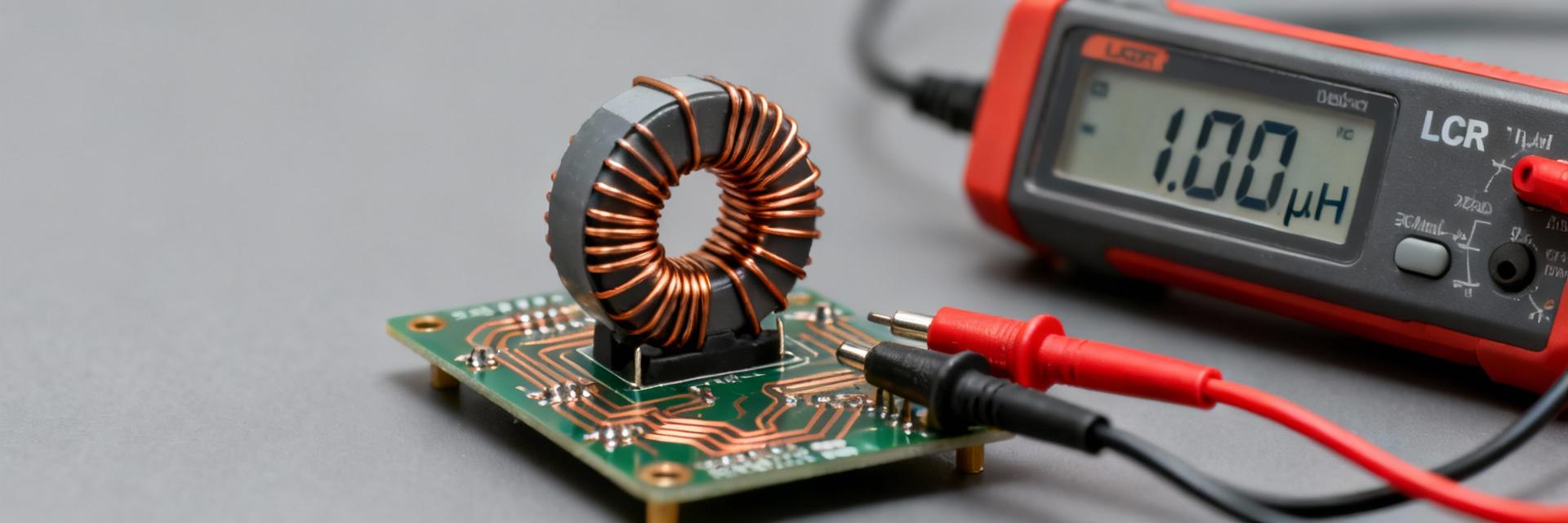
Explanation: extract rated current, DCR, and any thermal specs from the datasheet for inductor 784773156 to estimate steady dissipation; use those values to predict case rise and safe operating margins.
1.2 — PCB thermal fundamentals and metrics to track
Point: Board-level conduction and convection determine hotspot temperature, not the component alone.
Evidence: key metrics are thermal resistance (Rth), thermal impedance (Zth), delta-T above ambient, and rise time constant.
Explanation: a practical heat map and PCB thermal survey should report max board temp, Trise, and hotspot coordinates; report steady-state vs transient results so designers can judge derating and thermal cycling risk.
2 — Test & Measurement Methodology: Heat-Mapping Protocol
2.1 — Test-board design, instrumentation and test conditions
Point: Reproducible test results start with a controlled test board and documented setup.
Evidence: use a reference footprint for the part, defined copper pours and via stitching under pads, and controlled load steps (e.g., 0.25–1.0× rated current) in still air at 25°C ambient.
Explanation: instrument with an IR camera (≥640×480, 30–60 Hz), calibrated thermocouples near pad edges, and power measurement on input rails; provide a stepwise checklist so others can replicate power-in vs temperature curves.
2.2 — Data acquisition, processing and visualization best practices
Point: Measurement fidelity depends on emissivity, ROI selection, and temporal averaging.
Evidence: set camera emissivity to component finish, use thermal tape over small sensors for contact, and correct parallax by aligning camera normal to PCB.
Explanation: produce heat maps with consistent color scales, annotate hotspot coordinates relative to silk, export raw temperature grids for analysis, and document common errors (reflections, low-emissivity surfaces) with mitigation steps.
3 — Thermal Simulation & Model Verification
3.1 — Compact Thermal Model
Point: Simulations guide design changes when correlated to measurements.
Evidence: build a lumped Rth network for quick sensitivity runs and a transient CFD/FEA model for fidelity; include copper layer stackup, via stacks, and component dissipation as inputs.
3.2 — Correlation Analysis
Point: Correlation quantifies model reliability.
Evidence: align boundary conditions, tune contact resistances, and compare peak hotspot temps with RMSE and max ΔT as metrics.
Explanation: perform sensitivity studies varying copper area, via count, and convection coefficient; accept models where peak temperature error is within ±10% or an agreed ΔT threshold for design decisions.
4 — Case Study: PCB Heat Mapping Results for Inductor 784773156
4.1 — Visual results: annotated heat maps and hotspot analysis
Point: Heat maps reveal where board conduction limits occur and which nearby parts interact thermally.
Evidence: steady-state IR frames should show peak temp location relative to pad edges and copper pours, while transient frames capture Trise.
Explanation: annotate images with hotspot coordinates, overlay PCB artwork to show via placement, and caption images with "heat map" and "PCB thermal" context so engineers can quickly correlate artwork to thermal behavior.
4.2 — Quantitative metrics, risk assessment and reliability implications
Point: Translate measurements into actionable risk metrics.
Evidence: report input power, measured ΔT, inferred case temp, Zth, and time constant in a concise table.
| Input Power (W) | Measured ΔT (°C) | Inferred Case (°C) | Zth (°C/W) |
|---|---|---|---|
| 1.2 | 28 | 83 (≈181°F) | 23 |
Explanation: use inferred junction/case temps to determine derating and schedule reliability tests if margins are small.
5 — Design Recommendations & Mitigation Checklist
5.1 — Layout and cooling strategies to reduce hotspot temperature
Point: Targeted layout changes yield the largest thermal return on effort.
Evidence: via stitching beneath pads, expanding copper pours, relocating heat-sensitive parts, and orienting the inductor for better airflow typically lower hotspot temps by several °C in sensitivity studies.
Explanation: prioritize via stitching under the center pad, add thermal spoke pours tied to internal planes, and if allowable, add a small clip heatsink or thermal pad; note trade-offs in EMI and PCB cost.
5.2 — Validation checklist and re-test protocol
Point: A short re-test protocol confirms mitigation effectiveness.
Evidence: repeat the original test matrix, maintain identical ambient conditions, and compare peak temps and Trise before/after changes.
Explanation: acceptance criteria might be peak temp reduction ≥5–8°C or falling below the component derating threshold; document results and schedule thermal cycling if margins remain tight.
Summary
- Measure and map board hotspots with calibrated IR and thermocouples to quantify PCB thermal impact on the inductor 784773156; use consistent ROIs and color scales for comparison.
- Correlate a compact thermal model to heat maps with sensitivity runs on copper area and via count; target model peak-temp error within ±10% for design decisions.
- Mitigate hotspots by via stitching under pads, expanding copper pours, and relocating nearby heat sources; re-test against the documented checklist to verify reductions.
SEO & Publication Metadata
Frequently Asked Questions
What peak temperature should I expect for inductor 784773156 under rated load?
Typical peak depends on PCB layout and cooling; measured ΔT values in conservative layouts often put case temps near the 70–90°C range under moderate power. Use the test protocol to measure ΔT and infer case/junction temps from datasheet thermal resistance to determine derating margins.
How does PCB thermal strategy affect the lifetime of inductor 784773156?
Higher sustained operating temperatures accelerate insulation aging and magnetic material degradation. A well-implemented PCB thermal strategy — via stitching, copper redistribution, and reduced nearby heat sources — can lower hotspot temps several degrees, extending life and reducing the need for aggressive derating.
What is the recommended re-test protocol after layout changes to confirm PCB thermal improvements?
Repeat the original heat-map matrix at identical ambient conditions, record steady-state peak temps and Trise, compare against baseline, and apply acceptance criteria (e.g., ≥5°C reduction or peak below derating threshold). If margins remain tight, add thermal cycling and long-duration power soak tests.