A professional analysis of the 39 µH SMD power inductor performance characteristics for switching regulators and EMI suppression.
The 784773139 datasheet lists a 39 µH SMD power inductor with a 770 mA rated current and approximately 587 mΩ DC resistance. These numeric specs directly determine suitability in low‑power switching regulators and EMI suppression networks. This introduction gives a focused, data‑first reading guide so you can rapidly pull the relevant rows from the datasheet, compare tradeoffs between ripple handling and copper loss, and identify the mechanical and thermal checks to run before committing to prototypes.
Use this deep dive to extract the key performance indicators on the datasheet quickly: inductance and tolerance, DCR and copper loss, rated vs. saturation current, impedance vs. frequency curves, and the recommended footprint and reflow limits.
Quick overview: what the 784773139 datasheet tells you
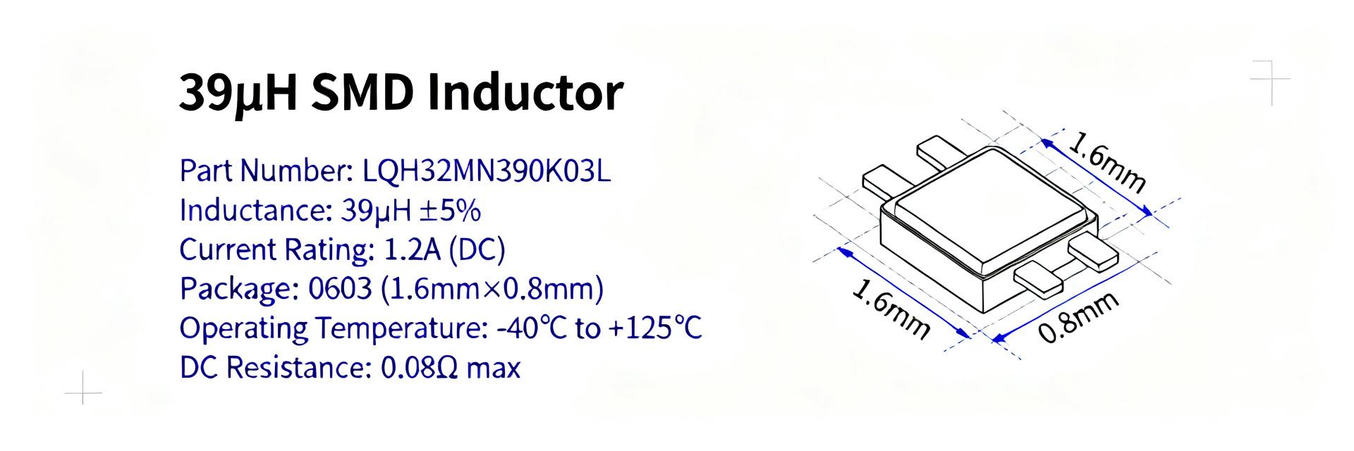
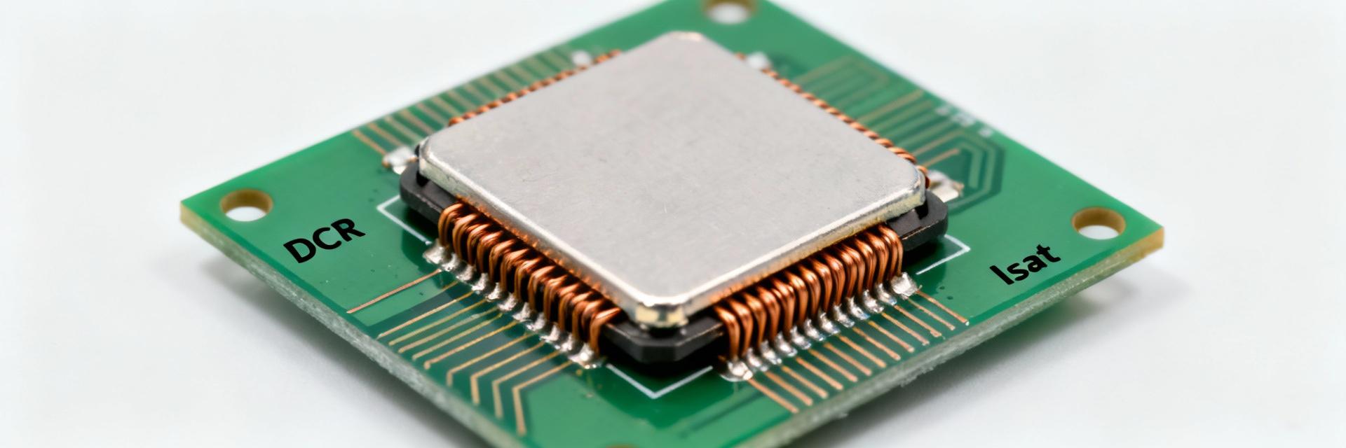
Part family & package type
Point: The datasheet identifies the part family and SMD package footprint that matter for placement and reflow.
Evidence: Typical datasheet sections show the part code, package outline drawing, and land pattern recommendation.
Explanation: Confirming the exact footprint ensures pad geometry, solder fillet formation and mechanical stability; mismatched footprints commonly cause weakened solder joints or tombstoning.
Typical target applications
Point: The 39 µH / 770 mA combination implies target use in low‑power DC‑DC converters and EMI suppression.
Evidence: The inductance is high relative to small buck chokes while the rated current is modest.
Explanation: Choose this part for higher L filtering at low switching frequency; pick a lower‑inductance, higher‑current part if ripple or saturation is a concern.
| Key Parameter | Datasheet Value | Design Impact |
|---|---|---|
| Nominal Inductance | 39 µH | Determines ripple current and energy storage. |
| Rated Current (IR) | 770 mA | Limits continuous load based on thermal rise. |
| DC Resistance (DCR) | ~587 mΩ | Directly affects copper loss (I²R). |
Electrical specifications breakdown
Inductance, tolerance and test conditions
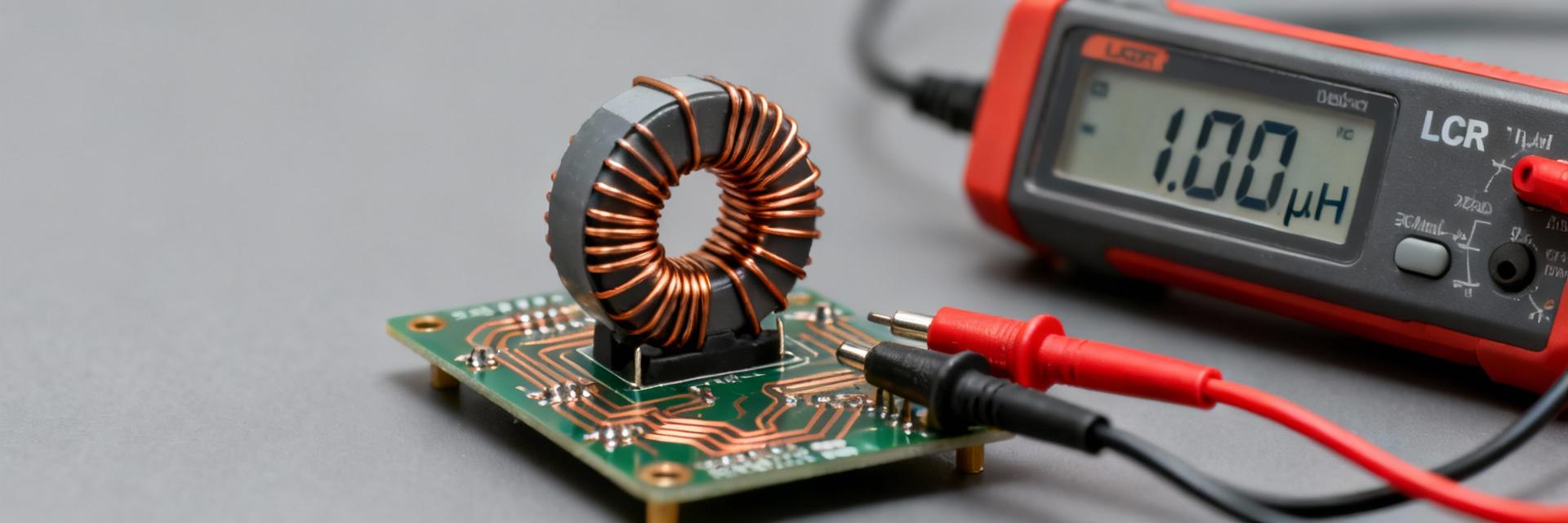
Point: Inductance value, stated tolerance and test conditions are primary specs to inspect. Evidence: Datasheets list the nominal 39 µH value with tolerance and the frequency and test instrument used. Explanation: Effective inductance at your switching frequency can differ; match test conditions or measure with expected DC bias to predict ripple.
Current ratings, saturation and DC resistance (DCR)
Point: Rated current, saturation current and DCR together define practical current handling and losses. Evidence: The datasheet separates a continuous rated current (770 mA) from a higher saturation figure and specifies DCR ~587 mΩ. Explanation: Use DCR to compute copper losses: P_loss = I^2 × DCR. For example, at 0.5 A, loss is 0.5^2 × 0.587 Ω ≈ 0.147 W.
Frequency and impedance behavior
Impedance vs. frequency and core/material implications
Point: Impedance vs. frequency plots reveal effective inductance and core losses across your switching band. Evidence: Datasheet curves show magnitude and phase vs. frequency. Explanation: Materials with higher permeability present higher impedance at low frequency but can saturate; unshielded designs may influence EMC.
Using datasheet curves for filter and power‑supply design
Point: Datasheet curves let you size L for ripple and estimate losses in a buck converter. Evidence: Calculate ripple current: ΔI ≈ Vsw / (L × f). Explanation: If impedance at the switching frequency is lower than nominal L suggests, expect larger ripple. Balance desired ΔI against I_rated and P_loss.
Mechanical, thermal and reliability specs
Mechanical drawings & Reflow: Follow the recommended land pattern to ensure correct solder fillet; adhere to the specified peak time and temperature in the reflow profile to avoid cold joints or thermal stress.
Thermal limits & Derating: Maximum operating temperature and derating curves determine allowable current in real environments. Combine computed P_loss and thermal resistance to maintain margin and lifetime.
Practical selection checklist and PCB design tips
- Component selection checklist: Validate inductance, tolerance, rated/saturation currents, DCR, and footprint match. Confirm alternate part codes and datasheet revision.
- Layout and test tips: Keep current loops short, isolate sensitive traces, and provide thermal relief. On the bench, measure inductance under DC bias and record temperature rise.
Summary
- The datasheet’s core numbers—39 µH inductance, 770 mA rated current and ~587 mΩ DCR—are the primary indicators for low‑power converter and EMI use.
- Use impedance vs. frequency curves to confirm effective inductance and predict ripple and insertion loss in filters or buck converters.
- Calculate copper losses (P_loss = I^2 × DCR) and combine with thermal limits to determine derating and safe continuous current on your PCB.
- Follow mechanical drawings and recommended land patterns closely and validate with bench tests—inductance under DC bias, temperature rise, and switching ripple.