Point: The 784773133 presents a compact, high-current solution with datasheet-highlighted ratings that make it suitable for modern point-of-load converters.
Evidence: Datasheet tables typically show a nominal inductance in the low‑microhenry range, single-digit milliohm DC resistance, and rated currents sized for multi-amp buck stages.
Explanation: This article delivers a concise spec breakdown, PCB footprint recommendations, selection guidance, and a hands‑on validation checklist so engineers can integrate the 784773133 into tight power rails with predictable thermal and electrical behavior.
Point: Readers will get actionable guidance rather than vendor marketing.
Evidence: The sections below cover identity, a compact spec table, frequency and thermal behavior analysis, land‑pattern advice, selection equations, and lab tests.
Explanation: Following these steps reduces rework risk during prototype cycles and speeds time to a validated power stage using this SMD power inductor.
1 — Product overview & core specs (background)
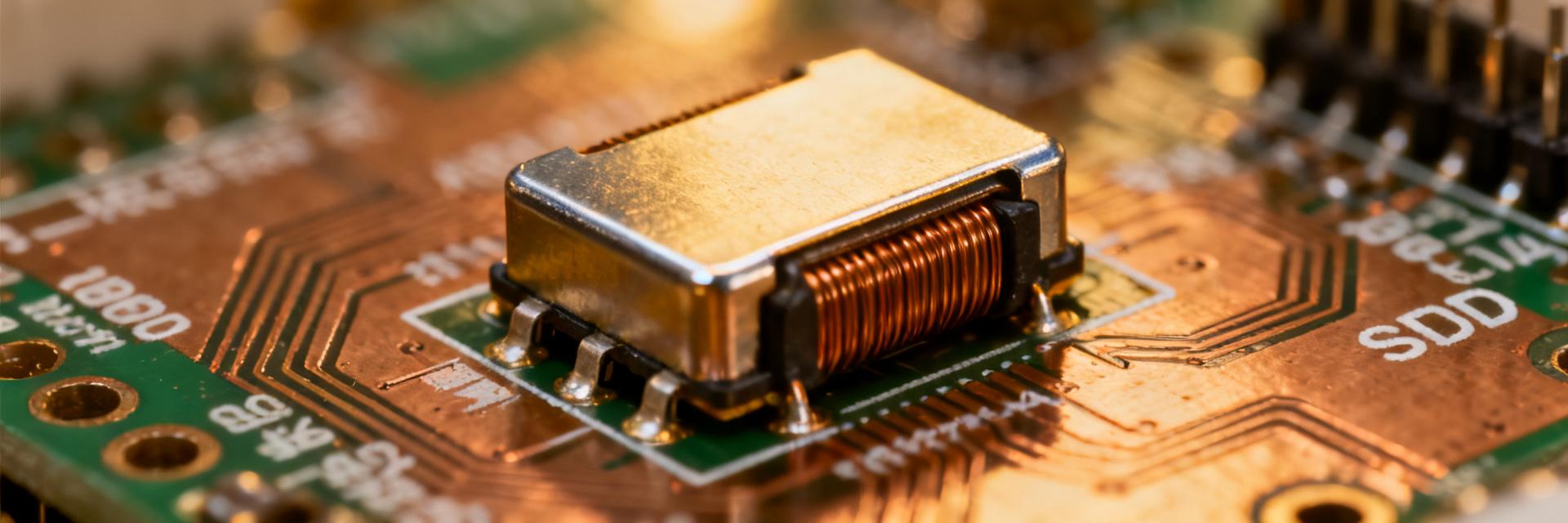
1.1 Part identity and primary function
Point: The component is an SMD power inductor intended for DC–DC converters and power rails; its role is to store energy and limit ripple current in switching regulators.
Evidence: Confirm sourcing by checking the full part number, package family designation, nominal inductance and tolerance, and rated current on the device label or procurement record.
Explanation: When sourcing, validate full part number, package code, inductance class, and current ratings to ensure electrical and mechanical interchangeability without depending on supplier names.
1.2 Quick electrical & mechanical summary (tab format)
| Parameter | Typical Value (example) |
|---|---|
| Nominal inductance | 1.0 µH |
| Tolerance | ±20% |
| DC Resistance (DCR) | ~8 mΩ |
| Rated current (thermal) | 8.0 A |
| Saturation current (L ≤ 70% nom) | 11.0 A |
| Operating temperature | -40 °C to +125 °C |
| Package dimensions (L×W×H) | 7.3 × 7.3 × 4.3 mm |
Point: Typical use cases include buck converters, synchronous regulators, and LC output filters. Evidence: The combination of low DCR and multi-amp ratings supports high-efficiency power stages. Explanation: Engineers should treat the table as a starting point and verify exact values against the official datasheet for final thermal and loop calculations.
2 — Electrical performance & ratings (data analysis)
2.1 Frequency response, inductance vs. current, and DCR behavior
Point: Inductance falls with increasing DC bias; this nonlinearity affects ripple amplitude and control-loop phase.
Evidence: Typical inductance-vs-current curves show a gradual decline up to rated current, with sharper drop near saturation current; impedance-vs-frequency plots show rising ESR and parasitic effects at high frequency.
Explanation: Include L vs I and impedance vs frequency plots during evaluation; use the reduced inductance at operating bias to recalc ripple and ensure the part avoids saturation in worst-case load transients.
Point: DCR increases with temperature, impacting conduction loss. Evidence: A DCR vs temperature curve often shows a linear rise with copper/trace heating; a low initial DCR minimizes I²R loss but does not eliminate temperature rise. Explanation: Account for DCR at expected operating temperature when computing steady-state losses and junction/ambient deltas for reliable thermal design.
2.2 Thermal limits, current ratings & derating strategy
Point: Differentiate rated current (thermal) from saturation current (magnetic). Evidence: The rated current is set so the component temperature rise stays within limits at a specified ambient and PCB copper; saturation current is where inductance falls below a defined percentage. Explanation: For continuous operation, derate to 60–80% of rated current depending on airflow and PCB copper; run thermal calculations using I²R losses plus convection assumptions to predict core temperature rise and copper requirements.
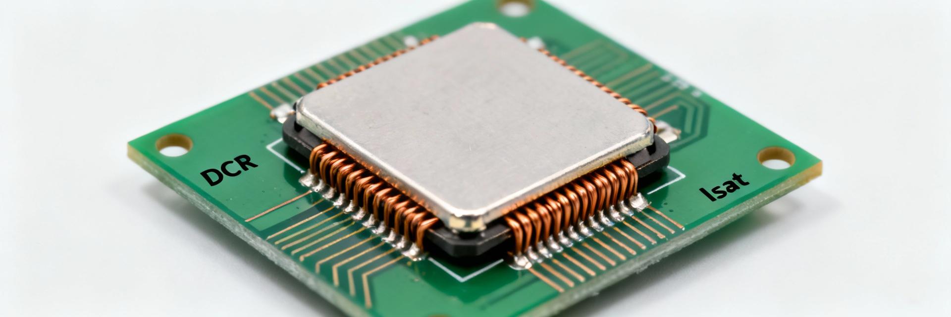
3 — Footprint & PCB layout (method / case)
3.1 Recommended land pattern and mechanical footprint
Point: A correct land pattern ensures solder fillet quality and consistent placement. Evidence: Recommended pad dimensions often match package terminals with small fillet zones and a solder mask defined escape to control paste. Explanation: Use the component outline drawing to set pad length, width, and spacing; a common land pattern for this package family is two rectangular pads sized to allow a 0.5–1.0 mm solder fillet, but verify exact numbers from the outline before generating the final footprint file labeled as the 784773133 footprint land pattern.
3.2 Thermal vias, copper pours, and assembly considerations
Point: Copper area and vias control temperature rise and current carrying capacity. Evidence: Adding pours on pads connected to heavy traces reduces trace temperature and spreads heat into internal layers; thermal vias can be placed near pads but not under magnetic cores unless approved. Explanation: For high-current layouts, connect pads to large copper pours with multiple thermal vias to inner planes, follow general SMT reflow profiles, and maintain placement keep-out for magnetic field clearance from sensitive analog routing. Include DFM/DFT checks for solder fillet inspection and X‑ray where necessary.
4 — How to select & integrate 784773133 in your design
4.1 Selection criteria: matching inductor specs to your converter
Formula Note: L = (Vin - Vout) * D / (ΔI * Fs)
Point: Selection follows a flow: required inductance, peak/continuous current, allowable DCR, switching frequency, and footprint constraints. Evidence: For a buck converter, required inductance L can be estimated from ΔI = (Vin - Vout) * D / (L * Fs). Explanation: Rearranged, L = (Vin - Vout) * D / (ΔI * Fs). Example: For Vin=12 V, Vout=3.3 V, Fs=500 kHz, D=0.275, and desired ΔI=30% of 8 A (2.4 A), L ≈ ((12-3.3)*0.275)/(2.4*500e3) ≈ 0.87 µH, indicating a 1.0 µH nominal choice fits typical designs.
4.2 Integration tips: EMI, stray inductance, and magnetics layout
Point: Minimize switching loop area and separate noisy nodes from sensitive traces. Evidence: Short, wide traces from switch to inductor and from inductor to output cap reduce EMI; placing input and output caps close to the switch node reduces radiated emissions. Explanation: Route return paths beneath switches, avoid routing analog reference traces adjacent to the inductor, and consider small shielding barriers or careful component orientation to mitigate coupling without vendor-specific shielding solutions.
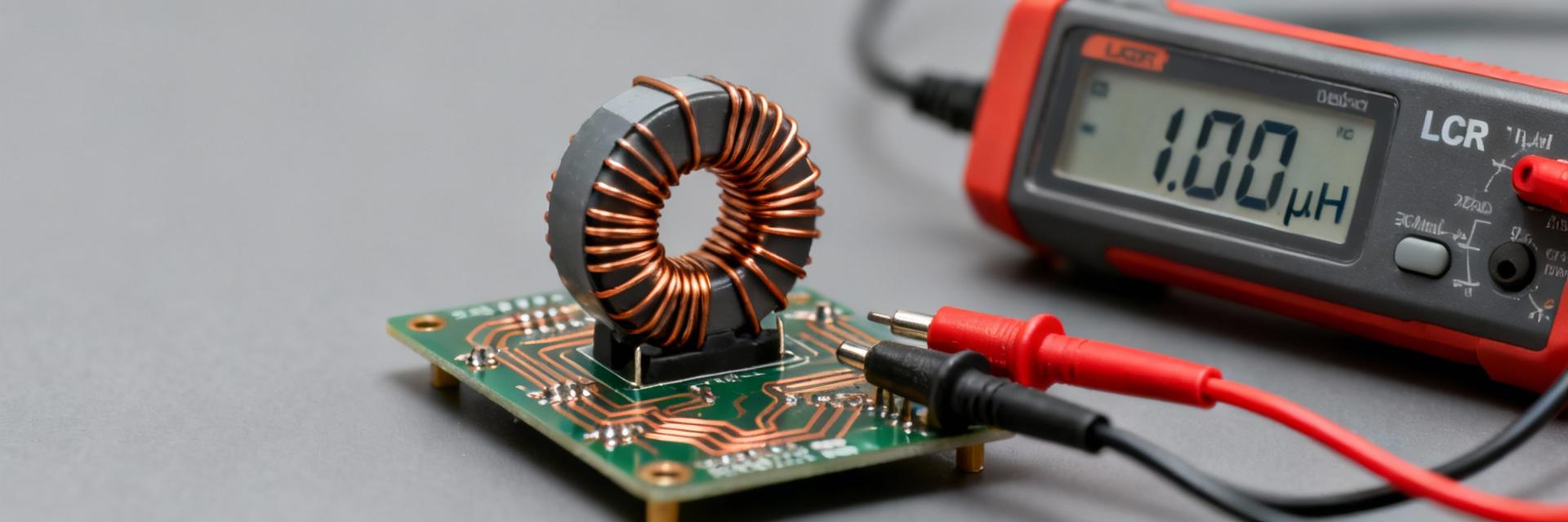
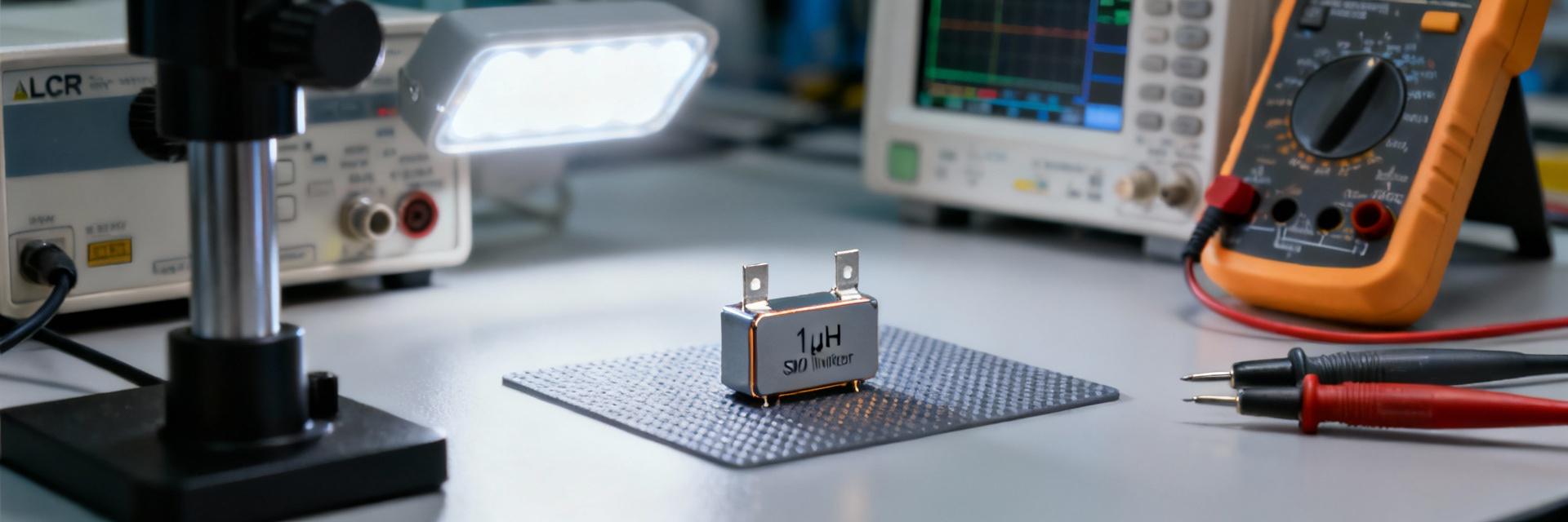
5 — Validation, testing & troubleshooting (action)
5.1 Prototype tests to verify performance
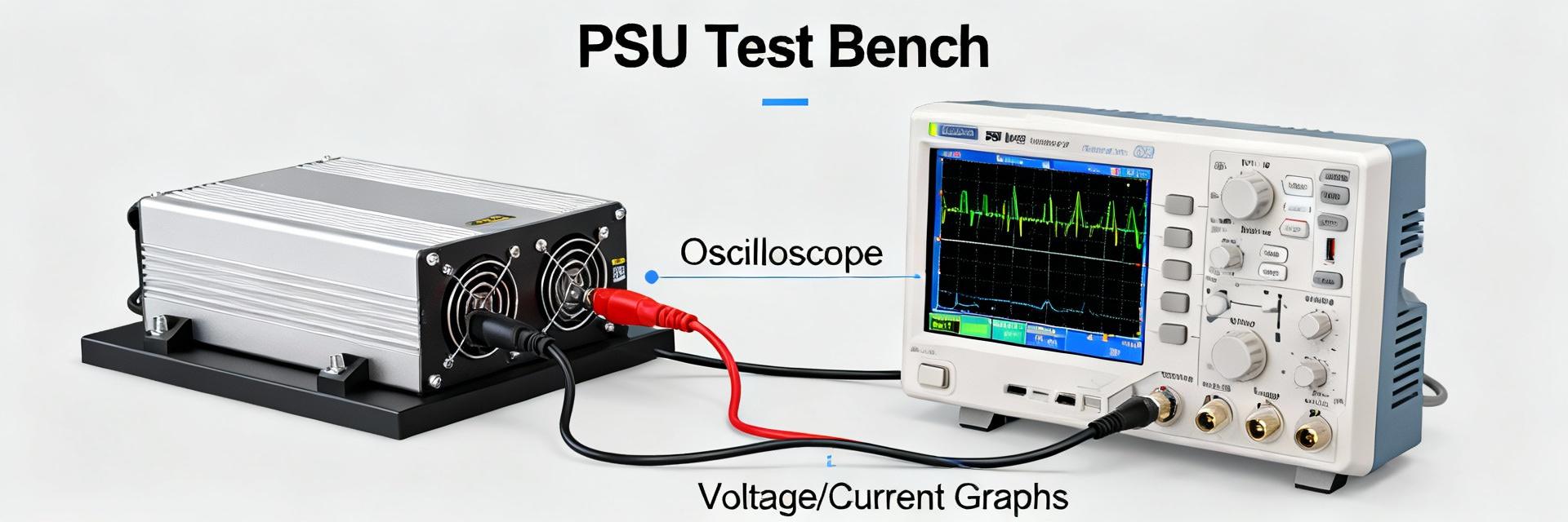
Point: Validate electrical and thermal behavior with targeted lab tests. Evidence: Recommended tests include L vs I sweeps, DCR measurement, thermal imaging under rated load, ripple measurement on the converter output, and impedance sweeps to reveal resonances. Explanation: Pass criteria: inductance within tolerance at operating bias, DCR consistent with datasheet at temperature, temperature rise within allowed limits, and output ripple below system spec. Use an LCR meter, thermal camera, scope with current probe, and network analyzer where available.
5.2 Common failure modes and fixes
Point: Typical failures are magnetic saturation, excessive heating, solder defects, and audible noise. Evidence: Saturation occurs under unexpected DC bias; heating stems from underestimated copper area or insufficient derating; solder issues appear as cold joints or tombstoning. Explanation: Troubleshoot by measuring inductance under bias, checking solder fillets and reflow profiles, increasing PCB copper or selecting a higher-rated part, and relocating the inductor to reduce thermal coupling or magnetic interference. Use the checklist: verify footprint, reflow profile, copper area, and bias current.
Summary Checklist
- Compact SMD Performance: Verify nominal inductance and DC bias behavior to ensure in‑circuit ripple targets with the 784773133.
- Footprint Strategy: Implement recommended land pattern, ample copper pours, and thermal vias to limit temperature rise.
- Selection & Integration: Compute required L from switching parameters, derate continuous current, and minimize switching loops.
- Validation: Measure L vs I, DCR at temperature, and perform thermal imaging under load.
Common questions
What should engineers check first when evaluating 784773133 for a buck converter?
First verify nominal inductance under expected DC bias and that rated current (thermal) and saturation current comfortably exceed peak and continuous load conditions; then confirm DCR and package fit for PCB constraints before prototype assembly.
How does inductance vs current affect converter design for a power inductor?
Inductance reduction under DC bias increases ripple and can shift control-loop dynamics; designers must use the inductance at operating current for ripple calculations and, if necessary, choose a higher nominal inductance or a part with better bias performance.
What are practical acceptance criteria during prototype testing?
Acceptance criteria include inductance within datasheet tolerance at operating bias, DCR consistent with thermal calculations, temperature rise within allowed bounds at rated current, and output ripple below your system target; failures should trigger layout, derating, or part selection revisions.